Behavior of the MSP430 CPU Core and System Clock at or Near 1.8 V
Explore how the MSP430's PMM-equipped, FRAM devices keep their CPU core and main system clock reliable and efficient even when your supply rail drops to 1.8 V.
by T.N. Krnich
Publish Date: July 2, 2025
Revision Date: July 2, 2025
MSP430 Microcontroller Journal is a Trademark.
Copyright © 2025 by Internetpress®
Introduction
This article focuses only on those members of the MSP430 family that include the Power-Management Module (PMM) and store their program in Ferroelectric Random-Access Memory (FRAM). In these devices the central processing unit (CPU) performs each instruction to the beat of the Main System Clock (MCLK), whose rhythm is usually set by the on-chip Digitally Controlled Oscillator (DCO). MCLK moves data through pipeline latches, advances the program counter, and times every peripheral transaction, while the DCO—guided by a Frequency-Locked Loop (FLL) tied to a low-frequency reference—holds its target frequency within a few parts per thousand. Because the DCO can wake and settle in mere microseconds, it is the oscillator of choice whenever the firmware demands an immediate return from sleep.
Origins of Power Supply Terms in Microcontroller Design
In electronic design, especially when working with microcontrollers like the MSP430, it’s important to understand a few foundational terms that appear again and again in datasheets, schematics, and firmware documentation. Among these are the phrase “power supply rail” and the acronyms DVCC, AVCC, DVSS, and AVSS. These terms are more than just labels—they carry with them a legacy of circuit design practices and help distinguish between different functional zones in a mixed-signal microcontroller.
The term power supply rail—often shortened to just “rail”—is a holdover from early days of circuit layout and remains in common use. It refers to the conductive paths that distribute voltage from the power source to various parts of a circuit. The word “rail” is metaphorical, conjuring up the image of a straight, continuous line. In early electronics, especially on breadboards or backplanes, power and ground lines literally ran down the sides of the board like a pair of rails, feeding multiple components along the way. On modern printed circuit boards (PCBs), these rails may take the form of wide copper traces or entire planes within the board layers, carrying regulated voltage across the system. Even though the form has evolved, the metaphor has remained, giving rise to common expressions like “the 3.3-volt rail” or “ground rail.”
The acronym DVCC stands for Digital Voltage at the Common Collector, and it refers specifically to the positive voltage supply rail for digital circuits inside the microcontroller. The “V” stands for voltage, while “CC” is a legacy abbreviation derived from bipolar junction transistor (BJT) terminology, where the collector of an NPN (Negative-Positive-Negative) transistor was tied to the positive supply in logic circuits. Historically, VCC described the positive rail in transistor-transistor logic (TTL), and the term has endured even as chip technology shifted to metal-oxide-semiconductor (MOS) designs.
Complementing DVCC is the term DVSS, or Digital Voltage at the Source to Source. Here, “SS” harks back to CMOS (Complementary Metal-Oxide-Semiconductor) technology, where the NMOS (N-type Metal-Oxide-Semiconductor) transistor’s source is usually connected to the lowest electrical potential—what we typically call ground. DVSS, then, identifies the ground or zero-voltage reference for digital logic blocks. Keeping this rail clean and stable is essential for predictable switching thresholds and reliable digital operation.
In systems that combine both digital and analog functions—like virtually every modern microcontroller—the analog subsystems often require separate power and ground rails to minimize electrical noise from digital switching. That’s where AVCC and AVSS come in. AVCC stands for Analog Voltage at the Common Collector, and supplies power to the analog circuitry: comparators, analog-to-digital converters, and voltage references. AVSS, or Analog Voltage at the Source to Source, is its corresponding ground. This partitioning allows analog blocks to ride on a quieter, less disturbed power domain, which improves measurement accuracy and signal fidelity.
“In MSP430 designs, the separation between DVCC/AVCC and DVSS/AVSS isn’t just bookkeeping—it’s a quiet shield for your analog signals against the chatter of digital logic.”
Understanding these terms makes it easier to read schematics, design PCBs, and write firmware that responds sensibly to power management events. More importantly, it lays the groundwork for grasping how microcontrollers like the MSP430 handle mixed-signal domains, low-voltage operation, and the practical realities of circuit noise. Even for engineers just getting started, this vocabulary opens the door to a deeper understanding of embedded power systems.
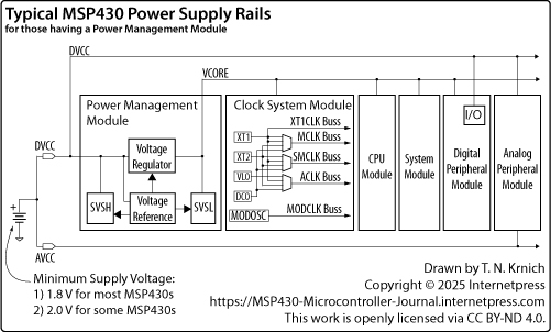
Typical MSP430 Power Supply Rails
Figure 1 shows a schematic view of the power supply rails used in currently produced MSP430 microcontrollers that include a Power Management Module (PMM). The diagram captures the internal layout of how power is distributed throughout the chip and offers a window into the power supply architecture now considered state of the art. These naming conventions and structural details reflect the present design direction taken by Texas Instruments, though the MSP430 is a platform under constant improvement—and both its terminology and internal configuration may evolve in future generations.
The diagram begins with a simple symbol for a battery, but that power source is merely representative. In practice, the external power can be any source that provides a stable voltage between 1.8 and 3.6 volts for most MSP430 devices. However, designers should take note: devices from the MSP430x5xx family and above often require at least 2.0 volts to fully activate specialized digital and analog peripherals. For low-power applications where the battery might drain to sub-volt levels—such as 0.5 volts—external regulation is required. A separate article will describe how to use high-efficiency step-up regulators to maintain the supply above the chip’s minimum threshold as the battery depletes.
From the external power supply, voltage enters the microcontroller through the DVCC and AVCC pins. These names stand for Digital VCC (DVCC) and Analog VCC (AVCC), and both are positive power rails. Each has a corresponding ground connection—Digital VSS (DVSS) and Analog VSS (AVSS)—though only the positive rails are shown in Figure 1. The earliest MSP430 chips used simpler naming, just VCC and VSS, but the naming evolved as analog and digital systems became more distinct within the chip.
The incoming DVCC rail directly feeds the PMM, which serves as the electrical heart of the device. The PMM contains a voltage regulator that steps DVCC down to a lower internal rail named VCORE. This internal supply rail powers the CPU core and all major system modules. The actual VCORE level varies by device and operating conditions, but for many MSP430s it is about 1.3 volts. This reduction allows the microcontroller to consume far less energy while still performing its digital functions.
The PMM isn’t just a regulator—it’s a set of coordinated circuits that supervise and stabilize the entire power environment. Its High-Side Supply Voltage Supervisor (SVSH) monitors the incoming DVCC supply before it reaches the regulator. Meanwhile, its Low-Side Supply Voltage Supervisor (SVSL) keeps watch on the regulator’s output—VCORE itself. Both supervisors reference an internal voltage standard generated by the PMM’s built-in voltage reference circuit. If DVCC or VCORE falls outside of safe limits, these supervisors can raise alarms. In many cases, those alarms trigger interrupts that prompt firmware to enter a safe low-power mode or issue a Power-Up Clear (PUC). If the voltage falls far enough, a Brown-Out Reset (BOR) may occur, forcing the microcontroller into a controlled restart. This orchestration ensures the CPU and memory never operate at voltages where logic gates might fail or data might flip unpredictably.
“The VCORE rail, created by the PMM’s internal regulator, reduces the chip’s core voltage to nearly 1.3 volts—sharply lowering power consumption without sacrificing performance.”
Once established, VCORE flows into the CPU and every major block: the system module, clock system, digital peripherals, and analog subsystems. The analog and digital peripheral modules also tap into the incoming DVCC rail, which powers circuits not driven by VCORE. Meanwhile, AVCC supplies the analog blocks with a cleaner, isolated voltage that avoids switching noise introduced by the digital power system. This distinction matters for subsystems like the Analog-to-Digital Converter (ADC) or Digital-to-Analog Converter (DAC), where noisy power lines can degrade precision.
The Clock System Module, shown between the PMM and CPU in Figure 1, is powered by VCORE. While this section will not go deep into its internal workings, it’s important to understand that every module in the MSP430 relies on clock signals for timing. No clock means no operation. Firmware can start or stop the system clocks by toggling control bits, allowing modules to sleep when inactive and resume quickly when needed. The clock busses shown in the diagram—MCLK, SMCLK, ACLK, and MODCLK—distribute timing signals across the chip to keep operations coordinated.
One small but important subsystem within the digital block is the General Purpose Input/Output (GPIO). The GPIO is shown in the figure as a sub-block labeled “I/O.” When configured as an output, a GPIO pin sources voltage from DVCC, making it capable of driving external LEDs, toggling control lines, or interacting with other circuits. In power-sensitive designs, keeping unused GPIOs in a known state can reduce leakage and save energy.
In sum, Figure 1 shows how the MSP430’s power supply is more than just voltage—it’s a carefully coordinated system of rails, regulators, supervisors, and references, all working together to maintain safe and efficient operation across a wide range of supply conditions.
How DVCC Becomes VCORE and why PMMCOREV Matters
The central processing unit’s core logic—the dense forest of flip-flops, multiplexers, and arithmetic blocks that executes each instruction—and the Digitally Controlled Oscillator (DCO) both draw power from the main on-chip rails: DVCC on the digital side and AVCC on the analog side.
Because those rails must serve everything from low-power peripherals to burst-current output drivers, the Power Management Module (PMM) inserts a precision point-of-load regulator in their path. This internal regulator trims DVCC down to a quieter, better-filtered line called VCORE, the private lifeline for the core logic and the clock generator.
How far the PMM drops DVCC is governed by the PMM Core Voltage Select bit-field (PMMCOREV) in the PMM control register. Each successive PMMCOREV code steps VCORE upward, giving the core more voltage headroom so it can switch faster when the firmware dials up the clock.
If the external supply drifts toward the MSP430's absolute minimum of 1.8 V, the PMM automatically forces PMMCOREV to its lowest code. That action preserves regulator headroom, keeps VCORE rock-steady, and ensures every gate inside the CPU continues to toggle cleanly. On the long-lived flash-based MSP430F5xx and MSP430F6xx families, this safeguard imposes a practical ceiling of 8 MHz for the Main System Clock (MCLK) at 1.8 V—an entry you will find in every Texas Instruments datasheet, dictated not by the core itself but by the extra time flash memory needs to deliver valid data when supply voltage is scarce.
FRAM: The Memory that Lets the Clock Run Free
Texas Instruments has been steering its newest MSP430 families away from flash and toward Ferroelectric Random-Access Memory (FRAM). A single FRAM cell flips state almost as quickly as static RAM, yet—unlike flash—it never calls on bulky on-chip charge pumps or time-consuming pre-erase cycles. From the silicon designer’s point of view, that means lower power overhead and a simpler, lighter voltage-regulation network inside the die.
For firmware developers the benefit is even more concrete: memory speed no longer drags on the system clock. In the MSP430FR5xx and MSP430FR6xx devices the Central Processing Unit (CPU) can stride all the way to 16 MHz at the minimum supply of 1.8 V, as long as the code sets the FRAM wait-state bit in the FRCTL (FRAM Control) register. Drop the clock to 8 MHz or below, clear that bit, and the core enjoys zero wait-state access—full efficiency at the very bottom of the voltage range.
The practical takeaway is that the choice of non-volatile memory sets the pace. Flash forces a hard ceiling on Master Clock (MCLK) because its slower write-and-erase physics dictate long wait states. FRAM, with near-SRAM performance, hands timing control back to the Digitally Controlled Oscillator (DCO); the memory system stops being the bottleneck, and the core can sprint as fast as the oscillator and voltage allow.
Holding the DCO on Target at Low Supply Voltage
The RSELx (Range Select) bits in the Basic Clock System Control Register 1 (BCSCTL1) choose which coarse frequency band the Digitally Controlled Oscillator (DCO) will occupy. Think of this setting as picking the right “gear” for the oscillator’s on-chip ring: with a higher RSEL value the DCO races faster, while a lower value slows it down so the core can still start up at the MSP430’s absolute minimum of 1.8 V.
Once the band is chosen, the tap field—formed by the five DCOx bits in the DCOCTL register—selects one of 32 taps around that ring, nudging the frequency in steps of roughly three percent. A second field, MODx, adds fractional dithering so the average can land midway between taps. Together, the tap value and modulation give fine-grain control without jumping to a new RSEL band.
Accuracy, however, is not left to guesswork. A small hardware state machine called the Frequency-Locked Loop (FLL) lives inside the clock module (BCS+ in legacy parts or the Unified Clock System in newer families). It counts DCO clock edges against a long-term reference—most often the 32 768 Hz watch crystal—and automatically tweaks the tap value until the tally matches, then repeats the comparison at regular intervals. In effect, the FLL turns the free-running DCO into a disciplined clock source whose long-term drift is bounded by the crystal.
That discipline matters even more when supply voltage droops. The DCO’s period shifts about two percent for every volt of VCC change, so a rail that slides down toward 1.8 V would otherwise pull the Main System Clock (MCLK) out of spec. Keeping the FLL enabled—or reopening it under firmware control for a quick retrim—re-anchors the oscillator to the crystal. With the DCO back on frequency, the Universal Asynchronous Receiver/Transmitter (UART) hits its target baud rate, timer tick intervals stay predictable, and sensor sampling windows open exactly where the application expects.
Guardians Against Deep Voltage Sags
Voltage rails in battery-powered projects can droop unexpectedly—an RF burst, a motor stall, or a cold morning may pull the cells below their nominal output. When that happens the Power-Management Module (PMM) posts two sentinels at the gate to keep the central processing unit safe.
The first is the Supply-Voltage Supervisor (SVS). Firmware programs the SVS with one of several coarse trip points that straddle the legal operating range of the Digital-Supply pin (DVCC). Whenever the rail crosses that trip point the SVS can raise an interrupt, buying the application a few microseconds to respond. Typical rescue maneuvers include throttling the Main System Clock, parking high-current peripherals, or diving into a low-power mode until the batteries recover. Because the SVS acts before real damage is done, the microcontroller retains context and can resume where it left off once voltage rebounds.
The second guardian is the Brown-Out Reset (BOR). Unlike the SVS, its trip level sits at a factory-trimmed, unmaskable threshold—usually around 1.55 V on modern FRAM parts and a few dozen millivolts lower on legacy flash devices. “Unmaskable” means the threshold cannot be disabled, lowered, or ignored by firmware; it lives in a tiny band-gap-referenced comparator that is always on. If DVCC ever undercuts that line the core is forced into a hardware reset, all registers revert to their POR values, and execution restarts only after the rail has climbed comfortably above the BOR point plus its built-in hysteresis. By clearing volatile state at the instant power becomes unreliable, the BOR prevents half-written data from corrupting flash or FRAM cells and guarantees deterministic start-up on the next rise of Vcc.
Texas Instruments includes both blocks in every MSP430 that carries FRAM and in all members of the MSP430F5xx and F6xx flash families. Working together, the SVS and BOR make certain that code never runs at voltages where bits might flip unpredictably—an invisible safety net that lets designers push their systems right to the 1.8 V edge without fear.
Summary
In short, within the PMM-equipped and FRAM-based ranks of the MSP430, the CPU core will run reliably at the low-voltage corner as long as the application respects each family's MCLK-versus-voltage curve, lets the FLL keep the DCO honest, and trusts the SVS and BOR to guard against the rare sag that falls below specification. With those guardrails in place, even a battery just shy of depletion can power a precise and responsive system clock.
Book Offer
References
- MSP430FR4xx and MSP430FR2xx Family User's Guide . Texas Instruments.
- MSP430FR57xx Family User's Guide . Texas Instruments.
- MSP430FR58xx, MSP430FR59xx, and MSP430FR6xx Family User's Guide . Texas Instruments.
- MSP430i2xx Family User's Guide . Texas Instruments.
- MSP430x1xx Family User's Guide . Texas Instruments.
- MSP430F2xx and MSP430G2xx Family User's Guide . Texas Instruments.
- MSP430x3xx Family User's Guide . Texas Instruments.
- MSP430x4xx Family User's Guide . Texas Instruments.
- MSP430x5xx and MSP430x6xx Family User's Guide . Texas Instruments.
- MSP430x09x Family User's Guide . Texas Instruments.
- CC430 Family Family User's Guide . Texas Instruments.
- RF430 Family User's Guide . Texas Instruments.
- RF430FRL15xH Family Technical Reference Manual . Texas Instruments.